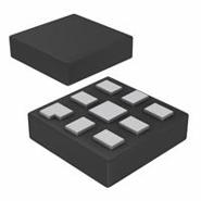
Image is for illustrative purposes only. Please refer to product description.
74LVC1G99GM,125
Configurable Multiple Function Surface Mount -40°C ~ 125°C Tri-State 74LVC 8-XQFN (1.6x1.6) 1.65 V ~ 5.5 V
- Product Category: Integrated Circuits (IC Chips)
- Mfr. Part # 74LVC1G99GM,125
- Manufacturer: NXP Semiconductors
- Package: 8-XFQFN Exposed Pad
- Lead Free Status /RoHS Status:
- Data Sheet: 74LVC1G99GM,125 Datasheet
- Inventory: In Stock
- Unit Price: Inquiry
- Quantity: -+
-
Please send inquiry,we will respond immediately.
Mfr. Part #: 74LVC1G99GM,125
- Specifications
- Product Details
Specifications
Product Details
General description
The 74LVC1G99 provides a low voltage, ultra-configurable, multiple function gate with 3-state output. The device can be configured as one of several logic functions including, AND, OR, NAND, NOR, XOR, XNOR, inverter, buffer and MUX. No external components are required to configure the device as all inputs can be connected directly to VCC or GND. The 3-state output is controlled by the output enable input (OE). A HIGH level at OE causes the output (Y) to assume a high-impedance OFF-state. When OE is LOW, the output state is determined by the signals applied to the Schmitt-trigger inputs (A, B, C and D).Due to the use of Schmitt-trigger inputs the device is tolerant of slowly changing input signals, transforming them into sharply defined, jitter free output signals. By eliminating leakage current paths to VCC and GND, the inputs and disabled output are also over-voltage tolerant, making the device suitable for mixed-voltage applications.
Features and benefits
â– Wide supply voltage range from 1.65 V to 5.5 Vâ– 5 V tolerant inputs for interfacing with 5 V logic
â– High noise immunity
â– Complies with JEDEC standard:
♦ JESD8-7 (1.65 V to 1.95 V)
♦ JESD8-5 (2.3 V to 2.7 V)
♦ JESD8-B/JESD36 (2.7 V to 3.6 V)
â– ESD protection:
♦ HBM JESD22-A114F exceeds 2000 V
♦ MM JESD22-A115-A exceeds 200 V
■±24 mA output drive (VCC = 3.0 V)
â– CMOS low power consumption
â– Latch-up performance exceeds 250 mA
â– Direct interface with TTL levels
â– Inputs accept voltages up to 5 V
â– Multiple package options
■Specified from −40 °C to +85 °C and −40 °C to +125 °C.
Â
ICCHIPS, where the pulse of innovation meets the heartbeat of wholesale excellence. Unveil the future of electronic components with our flagship product, the 74LVC1G99GM,125. As your conduit to groundbreaking technology, we stand as the bridge between visionary suppliers and pioneering manufacturers, committed to orchestrating seamless transactions that cater to the ever-evolving needs of the electronics industry.
Please send inquiry, we will respond immediately.
Mfr. Part #: 74LVC1G99GM,125


