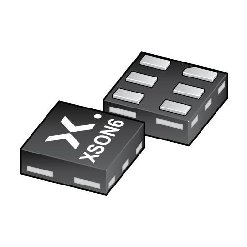
Image is for illustrative purposes only. Please refer to product description.
74LVCH1T45GS132
Bus Transceivers 74LVCH1T45GS/SOT1202/X2SON6
- Product Category: Bus Transceivers
- Mfr. Part # 74LVCH1T45GS,132
- Manufacturer: Nexperia
- Package: Cut Tape/Reel
- Lead Free Status /RoHS Status:
- Data Sheet: 74LVCH1T45GS,132 Datasheet
- Inventory: In Stock
- Unit Price: Inquiry
- Quantity: -+
-
Please send inquiry,we will respond immediately.
Mfr. Part #: 74LVCH1T45GS,132
- Specifications
- Product Details
Specifications
Product Details
General description
The 74LVC1T45; 74LVCH1T45 are single bit, dual supply transceivers with 3-state outputs that enables bidirectional level translation. They feature one data input-output port (A and B), a direction control input (DIR) and dual supply pins (VCC(A) and VCC(B)). Both VCC(A) and VCC(B) can be supplied at any voltage between 1.2 V and 5.5 V making the device suitable for translating between any of the low voltage nodes (1.2 V, 1.5 V, 1.8 V, 2.5 V, 3.3 V and 5.0 V). Pins A and DIR are referenced to VCC(A) and pin B is referenced to VCC(B). A HIGH on DIR allows transmission from A to B and a LOW on DIR allows transmission from B to A.The devices are fully specified for partial power-down applications using IOFF. The IOFF circuitry disables the output, preventing any damaging backflow current through the device when it is powered down. In suspend mode when either VCC(A) or VCC(B) are at GND level, both A port and B port are in the high-impedance OFF-state.
Active bus hold circuitry in the 74LVCH1T45 holds unused or floating data inputs at a valid logic level.
Features
■Wide supply voltage range:♦ VCC(A): 1.2 V to 5.5 V
♦ VCC(B): 1.2 V to 5.5 V
â– High noise immunity
â– Complies with JEDEC standards:
♦ JESD8-7 (1.2 V to 1.95 V)
♦ JESD8-5 (1.8 V to 2.7 V)
♦ JESD8C (2.7 V to 3.6 V)
♦ JESD36 (4.5 V to 5.5 V)
â– ESD protection:
♦ HBM JESD22-A114E Class 3A exceeds 4000 V
♦ CDM JESD22-C101C exceeds 1000 V
â– Maximum data rates:
♦ 420 Mbps (3.3 V to 5.0 V translation)
♦ 210 Mbps (translate to 3.3 V))
♦ 140 Mbps (translate to 2.5 V)
♦ 75 Mbps (translate to 1.8 V)
♦ 60 Mbps (translate to 1.5 V)
â– Suspend mode
â– Latch-up performance exceeds 100 mA per JESD 78 Class II
■±24 mA output drive (VCC = 3.0 V)
â– Inputs accept voltages up to 5.5 V
■Low power consumption: 16 μA maximum ICC
â– IOFF circuitry provides partial Power-down mode operation
â– Multiple package options
■Specified from −40 °C to +85 °C and −40 °C to +125 °C
ICCHIPS, where the pulse of innovation meets the heartbeat of wholesale excellence. Unveil the future of electronic components with our flagship product, the 74LVCH1T45GS132. As your conduit to groundbreaking technology, we stand as the bridge between visionary suppliers and pioneering manufacturers, committed to orchestrating seamless transactions that cater to the ever-evolving needs of the electronics industry.
Please send inquiry, we will respond immediately.
Mfr. Part #: 74LVCH1T45GS,132


